HOME > The Attractiveness of Kansai in Business > Companies Expanding Business in Kansai > Anjet Research Lab Co., Ltd.
Anjet Research Lab Co., Ltd.
Last update:April 7,2025
Company Overview
![]()
Parent Company Location: Taiwan
Japan Office Establishment: 2019
Location: 1-39 Goryo Ohara, Nishikyo-ku, Kyoto City, Kyoto University Katsura Venture
Plaza, South Building, Rm 2203
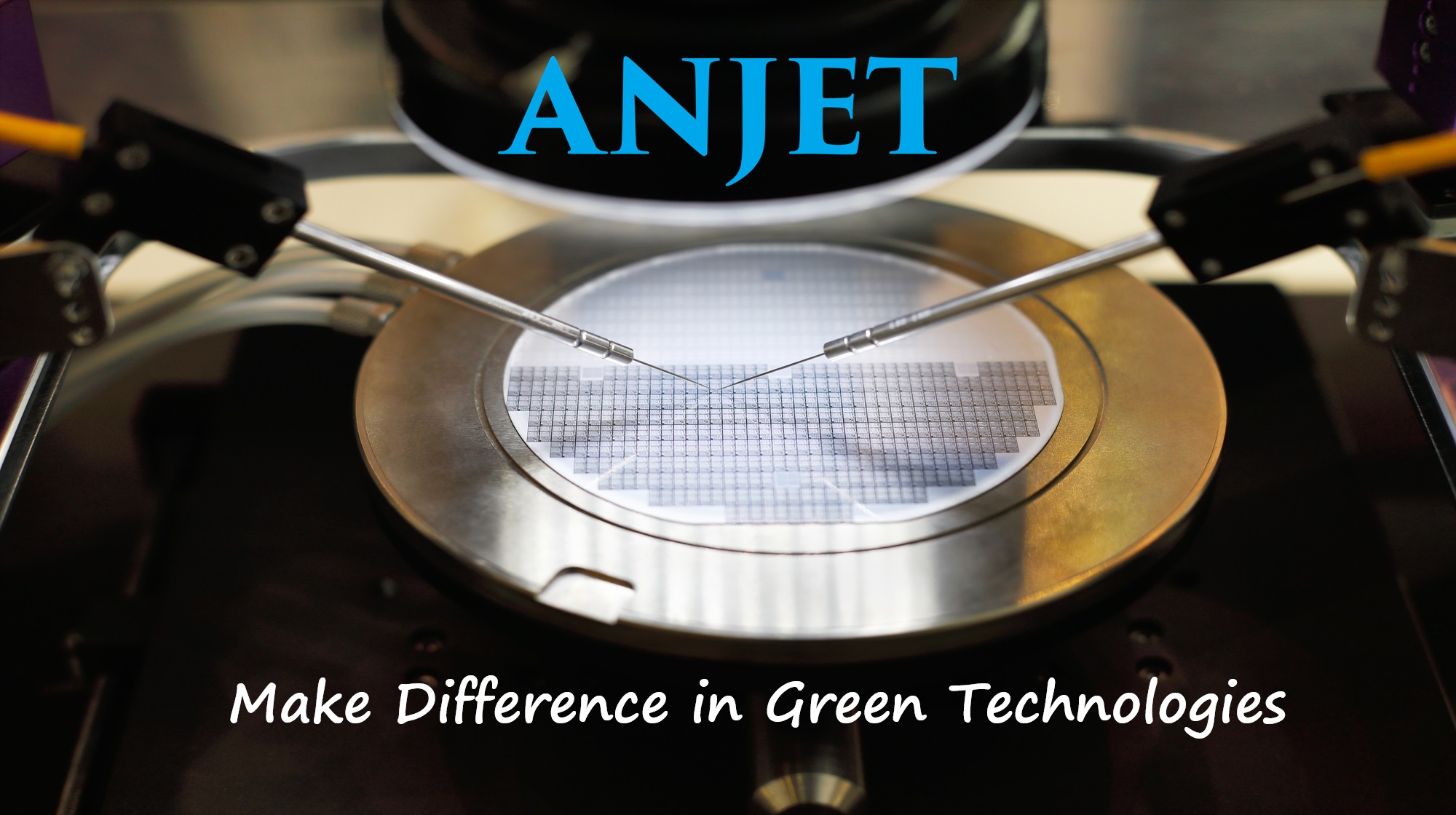
Business Activities: Design and development of semiconductor devices
Website: Anjet Research Lab Co., Ltd.
Interview
Anjet Research Lab Inc. is a startup founded in Kyoto in 2019, specializing in the design and development of next-generation power semiconductor devices. The company was established in response to Japan’s growing energy demand, driven by the rise of electric vehicles, renewable energy systems (such as solar and wind power), and data centers.
By combining Taiwan's advanced manufacturing technologies with Japan's high-level design expertise, the company develops high-performance power semiconductor devices that address industry needs such as efficient power conversion and thermal management.
We spoke with the company’s advisor, Mr. Kamisawa, about their expansion and the appeal of the Kansai region.
The Expansion into Kansai and the Appeal of Kyoto – The Semiconductor Industry and the Concentration of Knowledge
Currently, the demand for power semiconductors is rapidly increasing, and we predict this demand will continue to grow over the next 30 years.
Taiwan has a globally prominent presence in semiconductor manufacturing, while Japan excels in power semiconductor design and simulation. By combining the strengths of both countries, we established our company with the goal of expanding our business through a horizontal specialization.
This vision led to the founding of Anjet Research Lab Inc. by Jason Hsiao (Vice President) and Jimmy Wu (CEO), who were former colleagues at a semiconductor manufacturer in Kyoto.
Kyoto is home to many manufacturing equipment manufacturers with a global market
share, making it a major hub for the semiconductor industry. In addition, the region has a strong concentration of universities and research institutions, including Kyoto University, the Nara Institute of Science and Technology
(which is advancing research in compound semiconductors such as SiC and
GaN), Osaka University, and Ritsumeikan University—all easily accessible.
As a result, Kyoto is a region rich in both knowledge and human resources, spanning from modules and devices to fundamental material properties.
For a research and development-driven company like ours, which collaborates with universities and integrates cutting-edge academic research into product development, Kyoto provides an ideal environment. Furthermore, since our company was founded by colleagues who previously worked at semiconductor companies in Kyoto, it was a natural decision to establish our research base here.
In addition to its strengths in semiconductors, Kyoto is also active in bio-research, with numerous universities and research institutions advancing studies in this field. I believe this "concentration of knowledge" is a unique advantage of Kyoto as a region.
Public Support Utilized During Our Expansion
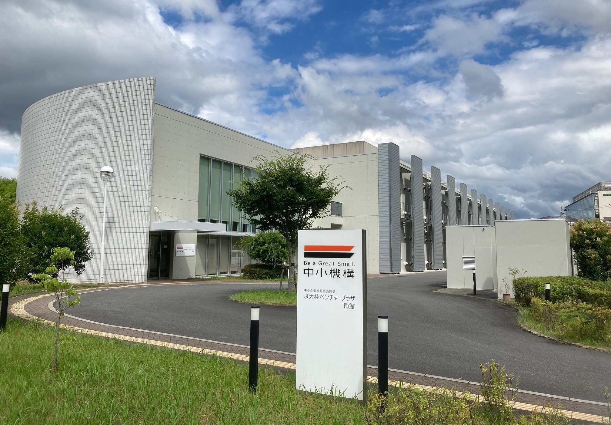
Kyoto University Katsura Venture Plaza
JETRO Kyoto(*): Support for business establishment procedures (opening bank accounts,
registration, property introductions, etc.)
(*)Please check the JETRO website for details.
SME SUPPORT JAPAN: Assistance with moving into incubation facilities
Kyoto City: Rent subsidies
As we were unfamiliar with the startup procedures, JETRO Kyoto provided
us with comprehensive support, enabling us to smoothly navigate the business
establishment process. Additionally, SME Support Japan helped us secure
a spot in an incubation facility. The "Kyoto University Katsura Venture
Plaza," where we are based, is adjacent to Kyoto University's Katsura
campus, offering significant advantage for industry-academia collaboration.
Furthermore, we also received rent subsidies from Kyoto City.
By leveraging these various forms of support, we were able to focus on launching our business while keeping initial costs low.
Future Plans
Having completed the development phase, we are now entering the stage of mass production. To achieve this, we plan to hire twice the number of engineers we currently employ.
Japan has many excellent design engineers, but in recent years, there has been a trend of these professionals moving abroad. At our company, we aim to attract talented engineers from across Japan to Kyoto, where they can contribute to creating high-quality power semiconductor devices for a sustainable energy society, thus providing next-generation energy solutions.
Message to Companies Considering Expansion
We believe that consulting with the JETRO Hong Kong office early on was a wise decision. Through that connection, we were introduced to JETRO Kyoto, SME Support Japan, and the local Kyoto government, which has provided continuous support since our establishment, offering advice on partnerships and human resources. We highly recommend relying on support organizations when expanding.
In Kyoto, the local government is also focused on supporting the semiconductor
industry. Currently, Kyoto Prefecture and City are collaborating to enhance
Kyoto’s presence in the global semiconductor industry by building a comprehensive
semiconductor ecosystem, from material research to semiconductor design,
production, and packaging. This initiative, the "Kyoto Semiconductor
Valley Concept," aims to strengthen industry-academia-government collaborations and attract highly
skilled global talent.
We feel that there is growing momentum in Kyoto to revitalize the semiconductor industry with a unified approach from industry-academia-government. For those with a background in the semiconductor field, it is an excellent environment, and for semiconductor companies considering expansion, Kyoto is undoubtedly the ideal location.
Contact Information
Ministry of Economy, Trade and Industry, Kansai Bureau
International Investment Promotion Division
Address: 1-5-44 Otemae, Chuo-ku, Osaka, 540-8535
Phone:+81-6-6966-6033
E-Mail:invest-japan-kansai@meti.go.jp![]()